|
|
Profile of Yoshihiro Hirota Yoshihiro Hirota was born in 1961 in Kyoto, Japan. He graduated from Kyoto Institute of Technology at 1985, and received a master’s degree from the same university at 1987, with his main study in atomic level crystal structure analysis with High-Resolution Transmission Electron Microscopy. After the graduating from the university, he joined in Sanyo Electric Co., Ltd. at 1987, and started his industry career mainly in CMOS device and process technology. He was working for the device development and process integration of 2.0~0.8 micro meter generation SRAMs and CMOS logic devices such as gate array device in the company. He jointed to Advance Technology Research Laboratories, Sumitomo Metal Industries, Ltd. at 1991. He worked for CMOS process design to develop some image processing LSIs, a CMOS imager and a test DRAM with a planar type capacitor to evaluate Si wafer quality in the company. He was offered to Innotech Corporation for photo pixel design and process integration of a unique CMOS imager with one ring gate MOSFET in 2000. At 2001, he joined to Tokyo Electron Ltd., and had been a group manager for FEOL process modules development. He worked for SPA, which stands for Slot Plane Antenna plasma process tool, application process development and for propagation of SPA products to customers widely between 2005 and 2009. He was a senior manager and working for FEOL process group leader, Leading edge Process Development Center between 2010 and 2016. He was a Project Leader, Memory Technology Project, and working for Device Technology Planning Dept. in HQ of Tokyo Electron Ltd between 2016 and 2021. He retired from Tokyo Electron Ltd. at September, 2021. He is Representative, Widevil now. And also he is a Program Cordinator, Kyoto Lab for a Greener Future, Kyoto Institute of Technology from September 2022 to now. He is also in charge of a part-time lecture in a class of the Graduate School of Electronic Systems, Kyoto Institute of Technology in 2024. |
||||||||||||||||||||||||||||||||||||||||
| Activities |
| 1. 2. 3. 4. 5. 6. |
Program Coordinator: Kyoto Lab for a Greener Future, Kyoto Institute of
Technolog Vice Chair: Program Committee, Electron Device Forum Kyoto, NEDIA Lecture: Electronic Device Training Course (Iintermediate Course), NEDIA Lecture: Summer/Winter Camp of The Planarization and CMP Technical Committee, The Japan Society for Precision Engineering Lecture: Autumn Seminer, Total Process Solution Study-Group Consultant: Tokyo Electron Limited. |
| Tutorial, lecture and Education etc. . |
| 1999年11月: 2014年5月: 2018年7月: 2019年5月: 2019年8月: 2019年9月: 2019年12月: 2020年3月: 2020年8月: 2020年12月: 2021年1月: 2021年5月: 2021年11月: 2021年11月: 2021年12月: 2022年5月: 2022年8月: 2022年11月: 2022年11月: 2022年12月: 2023年5月: 2023年9月: 2024年5月: 2024年6月: 2024年9月: 2024年10月: 2024年12月: 2025年1月: 2025年2月: |
ナノテスティング学会 ナノテスティングシンポジウム 国立交通大学(台湾) 招待講義 Open Tech Symposium 2018, Kyoto Institute of Technology パターニング戦略会議 2029 精密工学会・プラナリゼーションCMPとその応用技術専門委員会 サマーキャンプ 2019 SNIA日本支部 次世代不揮発メモリ分科会 2019 京都工芸繊維大学 半導体メモリデバイス特別講座 第67回応用物理学会春季学術講演会 招待講演(COVID-19, 出版のみ) 精密工学会 再招待(COVID-19,未実施) NEDIA、第1回 電子デバイス研修講座 (中級編) 26th ASP DAC (Asia and South Pacific Design Automation Conference): Tutorial NEDIA、第2回 電子デバイス研修講座 (中級編) 京都工芸繊維大学 半導体メモリデバイス特別講座 NEDIA、第3回 電子デバイス研修講座 (中級編) 精密工学会・プラナリゼーションCMPとその応用技術専門委員会・半導体デバイス製造技術基礎セミナー2021 NEDIA、第4回 電子デバイス研修講座 (中級編) 精密工学会・プラナリゼーションCMPとその応用技術専門委員会・CMP技術サマーキャンプ 2022 NEDIA、第5回 電子デバイス研修講座 (中級編) 京都工芸繊維大学、Home Coming Week 『工繊から社会へ』 精密工学会・プラナリゼーションCMPとその応用技術専門委員会・CMP技術ウインターキャンプ 2022 NEDIA、第6回 電子デバイス研修講座 (中級編) 精密工学会・プラナリゼーションCMPとその応用技術専門委員会・CMP技術サマーキャンプ 2023 NEDIA、2024年度 電子デバイス研修講座 (特別編B) 5月開催 JPCA、プリント配線板技術ロードマップ特別編セミナー 精密工学会・プラナリゼーションCMPとその応用技術専門委員会・CMP技術サマーキャンプ 2023 京都工芸繊維大学 『技術開発史』集中講義 「半導体デバイス温故知新」 大阪公立大学 2024年度 第11回『半導体デバイスプロセス技術基礎講座』 精密工学会・プラナリゼーションCMPとその応用技術専門委員会・CMP技術ウインターキャンプ 2024 NEDIA、2024年度 電子デバイス研修講座 (特別編B) 2月開催 |
 |
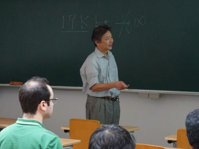 |
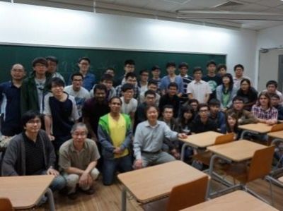
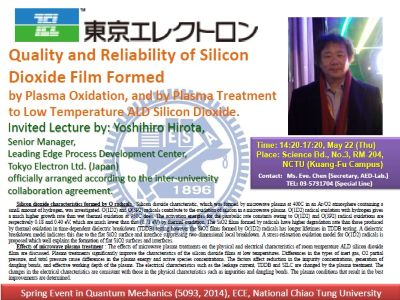
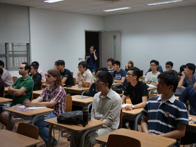
| 国立交通大学(台湾・新竹) 2014年 | 国立交通大学(台湾・新竹) 招待講義 2014年 |
 |
 |
| 国立交通大学(台湾・新竹) 招待講義 掲示 2014年 | 国立交通大学(台湾・新竹) 学生 2014年 |
| Publication |
Article
|
Abstract, Proceeding, Transaction of International Technology Conference
|
学会発表(国内)
|
| Patent |
| 国内特許出願 |
| No. | 文献番号 | 出願番号 | 出願日 | 公知日 | 発明の名称 |
| 1 | 特開2002-190536 | 特願2001-003960 | 2001/1/11 | 2002/7/5 | 半導体記憶装置、その製造方法及び半導体記憶装置の駆動方法 |
| 2 | 特許3283872 | 特願2001-114291 | 2001/4/12 | 2002/5/20 | 半導体記憶装置、その製造方法及び半導体記憶装置の駆動方法 |
| 3 | 特開2002-057536 | 特願2001-156862 | 2001/5/25 | 2002/2/22 | アナログ・インバータ回路 |
| 4 | 特開2001-324520 | 特願2001-054461 | 2001/2/28 | 2001/11/22 | インピーダンス検出回路、インピーダンス検出装置、及びインピーダンス検出方法 |
| 5 | 特開2001-124807 | 特願2000-260622 | 2000/8/30 | 2001/5/11 | 静電容量-電圧変換装置及び変換方法 |
| 6 | 特開2001-094408 | 特願2000-217324 | 2000/7/18 | 2001/4/6 | 静電容量型センサ、半導体製造装置および液晶表示素子製造装置 |
| 7 | 特開2001-091205 | 特願2000-217893 | 2000/7/18 | 2001/4/6 | 物体搭載装置 |
| 8 | 特開2001-035327 | 特願平11-208153 | 1999/7/22 | 2001/2/9 | 静電容量型近接センサ |
| 9 | 特開2000-304789 | 特願平11-110047 | 1999/4/16 | 2000/11/2 | インピーダンス/電圧変換装置 |
| 10 | 特開2000-304786 | 特願平11-110021 | 1999/4/16 | 2000/11/2 | インピーダンス/電圧変換装置及びその変換方法 |
| 11 | 特開2000-180498 | 特願平10-355947 | 1998/12/15 | 2000/6/30 | 半導体装置の評価方法 |
| 12 | 特開2000-055956 | 特願平10-226931 | 1998/8/11 | 2000/2/25 | 微小容量測定システム及びプロービングシステム |
| 13 | 特表2001-510580 | 特願平11-542367 | 1999/2/19 | 1999/8/26 | 容量検出システム及び方法 |
| 14 | 特表2001-525071 | 特願平11-542366 | 1999/2/19 | 1999/8/26 | 物理変量の検出装置及び方法 |
| 15 | 特表2000-514200 | 特願平11-540247 | 1999/1/22 | 1999/8/12 | インピーダンス-電圧変換装置及び変換方法 |
| 16 | 特表2000-515253 | 特願平11-538166 | 1999/1/22 | 1999/7/29 | 静電容量-電圧変換装置及び変換方法 |
| 17 | 特開平11-108975 | 特願平09-269847 | 1997/10/2 | 1999/4/23 | 容量/電圧変換回路及び容量変化検出型センサ装置 |
| 18 | 特開平11-023609 | 特願平09-179550 | 1997/7/4 | 1999/1/29 | 静電容量型センサ回路 |
| 19 | 特開平11-023608 | 特願平09-179549 | 1997/7/4 | 1999/1/29 | 静電容量型センサ回路 |
| 20 | 特開平10-190437 | 特願平09-255178 | 1997/9/19 | 1998/7/21 | レベルシフト回路 |
| 21 | 特開平10-074791 | 特願平08-231114 | 1996/8/30 | 1998/3/17 | 半導体装置 |
| 22 | 特開平10-009892 | 特願平08-185584 | 1996/6/26 | 1998/1/16 | センサ回路 |
| 23 | 特開平09-321228 | 特願平08-159019 | 1996/5/30 | 1997/12/12 | 半導体装置の容量素子の配線構造 |
| 24 | 特開平09-289286 | 特願平08-100953 | 1996/4/23 | 1997/11/4 | 半導体装置の容量素子 |
| 25 | 特開平09-145774 | 特願平07-305380 | 1995/11/24 | 1997/6/6 | デバイス劣化評価用半導体装置及びそれを用いたデバイス劣化評価方法 |
| 26 | 特開平09-082962 | 特願平07-240217 | 1995/9/19 | 1997/3/28 | 入出力保護回路 |
| 27 | 特開平09-074123 | 特願平07-226851 | 1995/9/4 | 1997/3/18 | 容量評価用半導体装置及び容量素子評価方法 |
| 28 | 特開平09-074122 | 特願平07-226850 | 1995/9/4 | 1997/3/18 | 半導体装置における容量測定パタ-ン及び容量測定方法 |
| 29 | 特開平08-181306 | 特願平06-318022 | 1994/12/21 | 1996/7/12 | MOS型半導体装置 |
| 30 | 特開平08-181081 | 特願平06-318023 | 1994/12/21 | 1996/7/12 | 半導体装置の製造方法 |
| 31 | 特開平08-055892 | 特願平06-193089 | 1994/8/17 | 1996/2/27 | 配線抵抗測定用半導体装置 |
| 32 | 特開平08-005706 | 特願平06-135599 | 1994/6/17 | 1996/1/12 | 劣化評価用半導体装置 |
| 33 | 特開平07-066400 | 特願平05-235820 | 1993/8/27 | 1995/3/10 | 半導体装置及びその製造方法 |
| 34 | 特開平07-066263 | 特願平05-211952 | 1993/8/26 | 1995/3/10 | 多層金属配線の接触抵抗測定方法並びに半導体装置及び半導体ウエハ |
| 35 | 特開平07-045697 | 特願平05-190252 | 1993/7/30 | 1995/2/14 | 半導体装置の製造方法 |
| 36 | 特開平07-029952 | 特願平05-171561 | 1993/7/12 | 1995/1/31 | 半導体装置及びこれを用いたアライメント検査方法 |
| 37 | 特開平06-268162 | 特願平05-055338 | 1993/3/16 | 1994/9/22 | 半導体装置及びその製造方法 |
| US Patents |
| No. | Pat No. | Priority | Filed | Published | Title |
| 1 | US8258571B2? | 2007/6/21 JP2007-164371 |
2008/6/20 | 2012/9/4 | MOS semiconductor memory device having charge storage region formed from stack of insulating films |
| 2 | US7161360B2 | 1999-07-22 JP20829599 |
2004/12/3 | 2007/1/9 | Electrostatic capacitance sensor, electrostatic capacitance sensor component, object mounting body and object mounting apparatus |
| 3 | US8318614B2? | 2007/3/26 JP2007079851 |
2008/3/25 | 2012/11/27 | Method for forming silicon nitride film, method for manufacturing nonvolatile semiconductor memory device, nonvolatile semiconductor memory device and plasma apparatus |
| 4 | US20110053381A1 | 2008/2/8 JP2008029478 |
2010/8/4 | 2011/3/3 | Method for modifying insulating film with plasma |
| 5 | US20120184107A1? | 2009/9/30 JP2009227638 |
2010/9/29 | 2012/7/19 | Semiconductor device manufacturing method |
| 6 | US7176706B2? | 2000/11/2 US09/703,845 |
2007/2/13 | 2007/2/13 | Capacitance measurement method of micro structures of integrated circuits |
| 7 | US20170287727A1 | 2014/9/25 JP2014-194963 |
2015/7/10 | 2017/10/5 | Metal hard mask and method of manufacturing same |
| 8 | US20140034893A1 | 2012/8/2 JP2012171839A |
2013/8/2 | 2014/2/6 | Switch device and crossbar memory array using same |
| 9 | US20140038430A1 | 2012/8/1 JP2012171107A |
2013/7/18 | 2014/2/6 | Method for processing object |
| 10 | US8241982B2? | 2008/5/9 JP2008-123561 |
2010/11/9 | 2012/8/14 | Semiconductor device manufacturing method |
| 11 | US7897498B2 | 2004/12/28 JP2004-380704 |
2005/11/29 | 2011/3/1 | Method for manufacturing semiconductor device |
| 12 | JP2005286314A | 2004/3/1 JP2004056629 |
2005/2/28 | 2005/10/13 | Method of separating resist film, rework method and device, and device for separating resist film |
| 13 | US20100176441A1? | 2007/6/7 JP2007-151265 |
2008/6/6 | 2010/7/15 | Semiconductor memory device and manufacturing method therefor |
| 14 | US20100140683A1 | 2007-03-26 JP2007-79852 |
2008/3/26 | 2010/6/10 | Silicon nitride film and nonvolatile semiconductor memory device |
| 15 | US8247289B2 | 2005-08-24 JP2005-243180 |
2006/8/23 | 2012/8/21 | Capacitor and manufacturing method thereof |
| 16 | WO2008123289A1 | 2007-03-26 JP2007079852 |
2008/3/26 | 2008/10/16 | Silicon nitride film and nonvolatile semiconductor memory device |
| 17 | EP1758152A2 | 2005-08-24 JP2005243238 |
2006/8/24 | 2007/2/28 | Capacitor and manufacturing method thereof |
| 18 | US20070184379A1 | 2004-03-01 JP2004-056629 |
2005/3/1 | 2007/8/9 | Peeling-off method and reworking method of resist film |
| 19 | JP2007055846A | 2005-08-24 JP2005243317A |
2005/8/24 | 2007/3/8 | METHOD OF FORMING DIELECTRIC FILM HAVING ABOx TYPE PEROVSKITE CRYSTAL STRUCTURE |
| 20 | US6326795B1? | 1998/2/19 JP10-078244 |
1999/2/19 | 2001/12/4 | Capacitance detection system and method |
| 21 | JP2001091205A | 1999-07-22 JP11-208294 JP20829499 |
2000/7/18 | 2001/4/6 | Object-loading apparatus |
| 22 | JP2002190536A | 2000/10/13 JP2000-313399 |
2001/1/11 | 2002/7/5 | Semiconductor storage device, manufacturing method and driving method thereof |
| 23 | JPH09145774A | 1995-11-24 JP7305380A |
1995/11/24 | 1997/6/6 | Semiconductor device for evaluating device deterioration and device deterioration evaluation method using it |
| 24 | US6034549A | 1996-10-30 JP28869696 |
1997/10/29 | 2000/3/7 | Level shift circuit |
| 25 | EP0972205B1 | 1998-02-05 JP2438498 |
1999/1/22 | 2006/12/13 | Impedance-to-voltage converter and converting method |
| 26 | JPH0982962A | 1995-09-19 JP7240217A |
1995/9/19 | 1997/3/28 | Input-output protective circuit |
| 27 | US5973538A | 1996-06-26 JP8-185584 |
1997/6/25 | 1999/10/26 | Sensor circuit |
| 28 | JP2001324520A | 2000-03-07 JP2000062504 |
2001/2/28 | 2001/11/22 | Impedance detection circuit, impedance detection device, and impedance detection method |
| 29 | JP2001035327A | 1999-07-22 JP11208153A |
1999/7/22 | 2001/2/9 | Capacitance type proximity sensor |
| 30 | EP0980004B1 | 1998-08-11 JP22693198A |
1999/8/11 | 2006/2/22 | Microscopic capacitance measurement system and probing system |
| 31 | JP2000180498A | 1998-12-15 JP35594798A |
1998/12/15 | 2000/6/30 | Operational amplifier circuit and method for evaluating semiconductor device |
| 32 | JPH0974123A | 1995-09-04 JP22685195A |
1995/9/4 | 1997/3/18 | Semiconductor device for capacitance evaluation and evaluation method for capacitor element |
| 33 | US10748782B2 | 2017-10-23 JP2017-204747 |
2018/10/19 | 2020/8/18 | Method of manufacturing semiconductor device |
| 34 | JPH08181081A | 1994-12-21 JP6318023A |
1994/12/21 | 1996/7/12 | Manufacture of semiconductor device |
| 35 | US8687405B2 | 2011-06-07 JP2011-127522 |
2012/6/4 | 2014/4/1 | Phase change memory and method for fabricating phase change memory |
| 36 | JPH0974122A | 1995-09-04 JP22685095A |
1995/9/4 | 1997/3/18 | Capacitance measuring pattern and its measuring method for semiconductor device |
| 37 | JP2009070919A | 2007-09-11 JP2007235733A |
2007/9/11 | 2009/4/2 | Plasma oxidation treatment method, and method of forming silicon oxide film |
| 38 | JP2000304786A | 1999-04-16 JP11002199A |
1999/4/16 | 2000/11/2 | Device and method for impedance/voltage conversion |
| 39 | JP2001124807A | 1998-01-23 JP10-11581 |
2000/8/30 | 2001/5/11 | Capacitance-voltage conversion device and conversion method |
| 40 | JP2007055845A | 2005-08-24 JP2005243272A |
2005/8/24 | 2007/3/8 | MANUFACTURING METHOD OF DIELECTRIC THIN FILM OF ABOx TYPE PEROVSKITE CRYSTAL STRUCTURE AND ITS MANUFACTURING UNIT |
| 41 | JPH11108975A | 1997-10-02 JP26984797A |
1997/10/2 | 1999/4/23 | Analog inverter circuit, capacity/voltage conversion circuit using the same and capacity change detection type sensor device |
| 42 | JP2000304789A | 1999-04-16 JP11004799A |
1999/4/16 | 2000/11/2 | Impedance/voltage converter |
| 43 | JPH0766400A | 1993-08-27 JP23582093A |
1993/8/27 | 1995/3/10 | Semiconductor and its manufacture |
| 44 | JPH1074791A | 1996/8/30 JP8231114A |
1996/8/30 | 1998/3/17 | Semiconductor device |
| 45 | JPH0766263A | 1993-08-26 JP21195293A |
1993/8/26 | 1995/3/10 | Contact resistance measuring method of multilayered metal wiring, semiconductor device and wafer |
| 46 | JPH0729952A | 1993/7/12 JP17156193A |
1993/7/12 | 1995/1/31 | Mos semiconductor device and alignment inspection by use of same |
| 47 | JPH0855892A | 1994/8/17 JP19308994A |
1994/8/17 | 1996/2/27 | Semiconductor device for measuring wiring resistance |
| 本サイト内の文章・写真・その他著作物の無断複製・転載を禁じます。 Widevil Copyright© 2014-2025 Widevil. All Rights Reserved |